

Nanostructures such quantum dots fabricated on modulation-doped AlGaAs/GaAs heterostructures are widely used in spin-based approaches to quantum computing. Charge noise in these devices, however, limits gate fidelity. A quiet electrostatic environment is therefore essential for further progress.
It is known that one major contribution to charge noise is the tunneling of electrons from the surface gates to the 2D electron gas via intermediate trap sites. In order to reduce this tunneling, our research is focused along two lines. First, we are examining new heterostructure designs and fabrication recipes in which we attempt to reduce both the ease of tunneling from the surface as well as the density of traps in the modulation doping layer. Second, we are also investigating undoped, accumulation-mode heterostructure designs since it is believed that Si donors in the modulation doping layer could mediate electron tunneling from the surface. Since these accumulation mode devices necessarily require the use of dielectric layers, one major thrust of the project is to compare the noise level in devices with different dielectric materials and deposition methods.
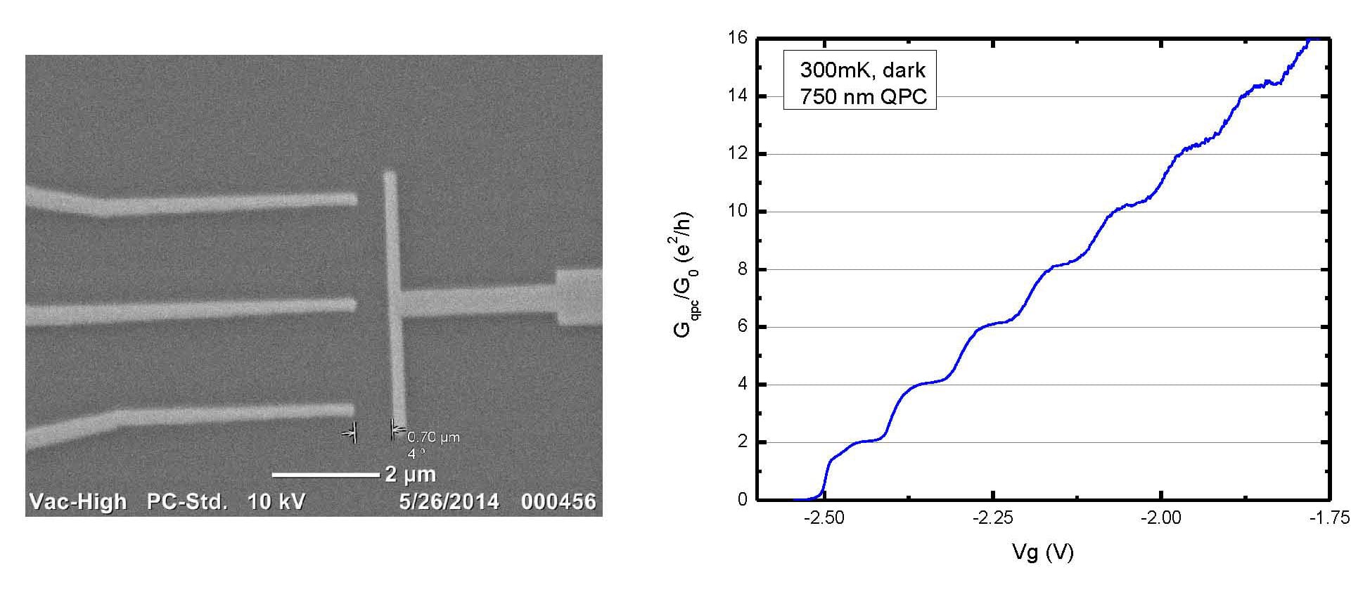
The charge noise is characterized using laterally defined quantum point contacts (QPCs) to detect charge fluctuations by operating the QPC in transition regions between neighboring conductance plateaus where the conductance is very sensitive to the local electrostatic environment. By monitoring current fluctuations in these devices, we can then quantify the noise level and make meaningful comparisons between different heterostructure designs and device fabrication recipes.

