

The Quantum Semiconductor Systems group studies the behavior of electrons confined in reduced dimensional systems subject to strong mutual interactions. Researchers in the Quantum Semiconductor Systems group use a variety of techniques including semiconductor growth by molecular beam epitaxy (MBE), nanofabrication and low-temperature transport to explore this exciting field. MBE is a process to fabricate crystalline semiconductor heterostructures for the study of novel physical properties and solid-state device technology. In an MBE system we can grow heterostructures of dissimilar materials with atomic monolayer resolution. This allows us to explore the properties of strongly interacting electrons in two dimensions. We also utilize the nanofabrication facilities at the Birck Nanotechnology Center to further confine electrons in 1D (quantum wires) and 0D (quantum dots) structures. These reduced dimensional systems exhibit many emergent phenomena that may find applications in quantum computing. The Quantum Semiconductor Systems group uses electrical transport experiments at temperatures down to T=10mK and magnetic fields up to 15Tesla to interrogate the samples we create. We also use MBE to pursue novel light-emitting sources in the Al(In)GaN heterostructure system. You will find brief descriptions of our ongoing projects below.
 Quantum Computing with Majorana Fermions in Hybrid Semiconductor/Superconductor Systems
Non-abelian Majorana zero modes (MZMs) in hybrid superconductor-semiconductor system promise information processing robust to decoherence. The combination of a high spin-orbit semiconductor and an s-wave superconductor, submitted to an in-plane magnetic field, is predicted to host such MZMs and serve as a platform for topological quantum computation. Read more →
 Non-Abelian Phases in the Fractional Quantum Hall Regime
The fractional quantum Hall effect (FQHE) occurs in a two-dimensional electron gas (2DEG) subjected to a perpendicular magnetic field at low temperature. It is now understood to arise from strong electron-electron interactions. In transport experiments the FHQE is characterized by Hall resistance quantized to rational fractional values of h/e2 and vanishingly small longitudinal resistance. Quasi-particle excitations in the FQHE are called anyons. Read more →
 Probing integer and fractional quantum Hall states in electronic interferometers
The fractional quantum Hall states are predicted to host exotic quasiparticles carrying fractional charge and obeying anyonic braiding statistics. It has been proposed that these properties may be observed through interference experiments. Our efforts focus on fabricating electronic Fabry-Perot interferometers on ultra-high quality GaAs wafers in order to probe fractional charge and statistics. Read more →

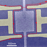
Engineering Heterostructures for High Fidelity Spin Qubits
Nanostructures such quantum dots fabricated on modulation-doped AlGaAs/GaAs heterostructures are widely used in spin-based approaches to quantum computing. Charge noise in these devices, however, limits gate fidelity. A quiet electrostatic environment is therefore essential for further progress. Read more →
Image courtesy of Ferdinand Kuemmeth.
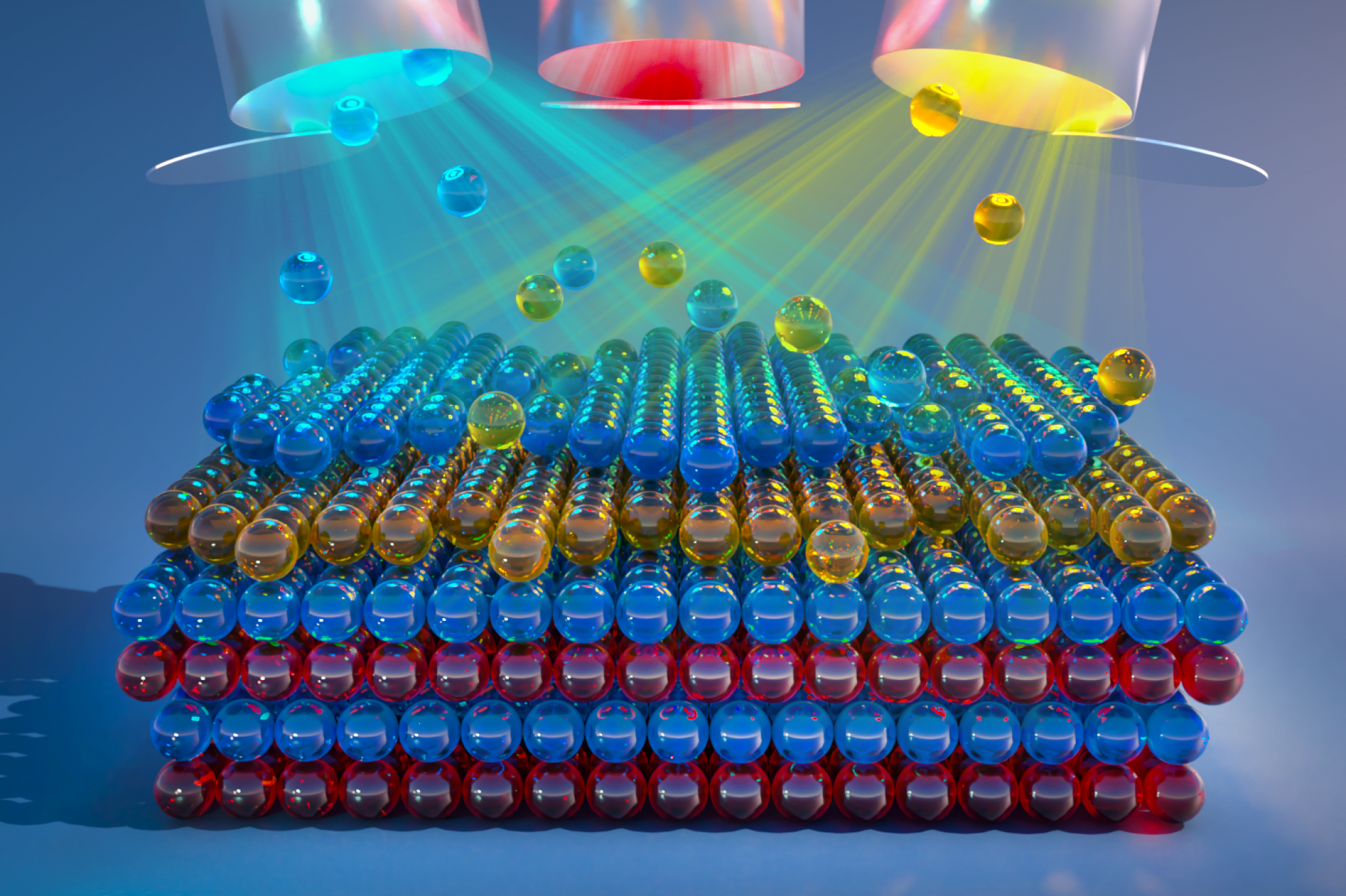
 Ultra-High Mobility 2DEGs and 2DHSs in GaAs Grown by Molecular Beam Epitaxy
A major thrust in the Quantum Semiconductor Systems group is growth of extremely high quality GaAs/AlGaAs heterostructures. One metric of quality is 2D mobility, which can now exceed 30 x 106 cm2/Vs at low temperatures. At low temperature mobility is limited by imperfections in the grown sample. Imperfections include intentionally introduced charged impurities, unintentional background charged impurities and structural defects.
Our efforts are focused in 3 areas: improved MBE vacuum conditions, source material purity, and heterostructure design. Read more →
 Novel Devices with Non-Polar m-plane GaN/AlGaN and Lattice-Matched AlInN/GaN heterostructures
Our work in the III-Nitride material system is focused on exploiting its unique physical properties to produce novel light sources based on intersubband transitions. Due to the large conduction band offsets available in Al(In)GaN/GaN heterostructures, intersubband transitions can span the technologically important near-IR (~1.5microns) to far-IR (~100microns) spectral range. Read more →